SI-C33DSP
An economical Digital Signal Processor (DSP) card for the PCI bus
The SI-C33DSP-PCI from Sheldon Instruments is a powerful Digital Signal Processor (DSP) card for your PC equipped with a PCI bus. It is based on Texas Instruments’ new 150Mhz TMS320VC33, 32 bit floating point DSP, and can transform your PC into an ultra high performance development system and DSP accelerator.
C3x devices supported on the SI-C33DSP card:
TMS320VC33
A full line of software development tools are available from Sheldon Instruments and TI, which include compilers, assemblers, linkers, and debuggers.
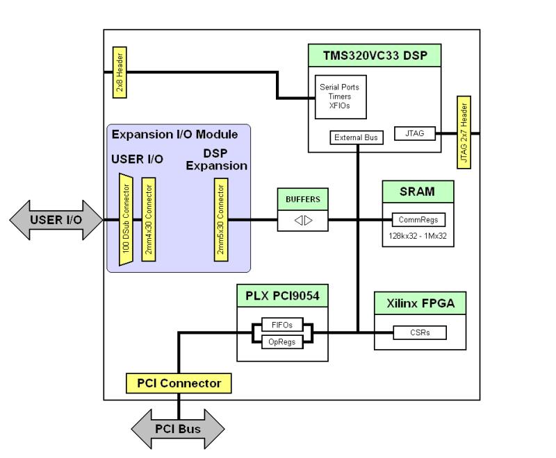
Host PCI bus to DSP Link
All communication between the host and the DSP take place by means of PLX’s PCI 9054 IC. Three (3) methods may be used for data transfer between the PCI bus and the DSP’s memory: 1) dual access mode, 2) PCI initiated bus mastered transfer mode with the 9054 acting as the bus master, and 3) bus mastering with the DSP acting as the PCI bus master.
For the dual access mode, all of the DSP’s zero wait state SRAM memory is simultaneously accessible by both the PCI bus and the DSP with the 9054 behaving as a target peripheral. The DSP’s memory is directly mapped into the first target region of the 9054, which can be accessed with standard memory access calls.
Onboard control logic arbitrates the appropriate timing between the C33’s primary bus, the SRAM, and the 9054’s Local bus. This is accomplished by asserting the C33 HOLD signal for no more than three (3) of its own clock cycles, every time the PCI side performs an access.
In addition to the dual access memory, large blocks of data can be transferred using PCI bus master transfers. The first bus master transfer method involves using the 9054’s DMA capabilities to access the DSP memory. The second bus master transfer method allows the DSP to act as the PCI bus master, where it actually has direct access to the host computer’s main memory! Both PCI bus master methods may allow for the highest possible burst transfer rates to take place over the PCI bus without host processor intervention.
Hardware Expansion
The SI-C33DSP-PCI includes expansion connectors allowing for custom designs, or for attaching ‘off the shelf’ multifunction I/O modules from Sheldon Instruments. Sheldon Instruments offers several daughter modules for multichannel analog and digital I/O, including 4 to 64 channels of 16 bit ADCs and DACs.
The SI-C33DSP-PCI is available with extensive development tools from Sheldon Instruments and TI.
For quick turnkey development, Sheldon Instruments offers QuVIEW and QuBASE, which are a set of DSP-resident libraries for real time performance that greatly accelerate data acquisition, signal processing, and control applications. QuVIEW is a real time accelerator for LabVIEW, and QuBASE a real time accelerator for Visual Basic. A full range of examples and tutors are provided to demonstrate their ease of use and breadth of functionality and capabilities. QuBASE runs under Windows, while QuVIEW also runs under Linux.
Typical benchmarks for a 150Mhz C33 processor include the computation of a 1024 point Radix-2 complex FFT at 400us.
When purchased as a DSP evaluation board, Sheldon Instruments also includes free sample DSP and Windows or Linux 32/64 bit device driver source code to accompany TI’s CCS development environment. The DSP source code illustrates full communication modes, and the Windows or Linux 32/64 bit device driver source code includes the complete SI-DDK, along with COFF file loader utilities.
Processor for SI-C33DSP
[table class=”siTB”]
TI 75MHz TMS320VC33[attr colspan=”2″]
MFLOPS, 150
DMA Channels, 1
Internal SRAM, 34K x 32 bit words zero (0) wait state SRAM
[/table]
External Memory
[table class=”siTB”]
SRAM Memory[attr colspan=”2″]
Sizes[attr rowspan=”2″], 512k x32
1M x 32
Type/Speed, one (1) wait state dual access SRAM running at 75Mhz
[/table]
Interfaces
[table class=”siTB”]
PCI Interface between Host PC and DSP[attr colspan=”2″]
Active Communication Modes[attr rowspan=”2″], Data Transfers: Bus master DMA and target mode
Messaging with user defined mailboxes
Transfer Rates[attr rowspan=”2″], Burst Transfers: Up to 132Mbyte/sec with block sizes of eight (8) 32 bit words
Sustained Transfers: Up to 12Mbyte/sec with any block size using DMA
[/table]
Connectors
[table class=”siTB”]
Port Connectors[attr colspan=”2″]
PCI, Desktop PCI: One Edge connector
JTAG, One 14 pin (2×7) header
GPIOs & Timers, One 16 pin (2×8) header: Serial Port 0 – XF[1:0] – TMCK[1:0]
DSP Primary Bus, One 120 pin (2mm 4×30) Peripheral Expansion connector
[/table]
[table class=”siTB”]
Peripheral Expansion[attr colspan=”2″]
DSP Expansion[attr rowspan=”2″], First external 2mm pitch: 120 pin (4×30) socket connector for interfacing the expansion module to the DSP’s primary bus
DSP Primary bus: Isolated using LVC2245 buffers. Decodes 64kx32 words mapped from 0xFE0000-0xFE1FFF Address (A[15:0]); Data (D[31:0]); Control (X_R/Wn – X_CSn – X_INT[1:0] – X_RDY – X_CLK[1:0]); and Power (3.3V; +/-12V; 5V; 1.8V)
User I/O[attr rowspan=”2″], Externally accessible user I/O 100 pin connector: half pitch (0.050″); Series III DSUB for interfacing external user defined signals to the 2mm User I/O connector. AMP part 787169-9; 787170-9; or 787362-9
Second external 2mm pitch: 120 pin (4×30) socket connector for interfacing external user defined signals to custom daughter module. Linked only to externally accessible 100 pin half pitch DSUB connector
[/table]
Mechanical Properties
[table class=”siTB”]
Physical Dimensions/Electrical Requirements/Temperature[attr colspan=”2″]
Form Factor Dimensions, Desktop PCI (1/2 size): 6.4″/16.26cm(L) x 3.9″/9.9cm(W)
Weight, 0.31lbs/140 grams
Supply Voltages, +3.3Vdc @ 0.5A; ±12Vdc supplies passed on to expansion connector and not used by onboard circuitry
Power, 1.5 Watts typical with 512Kx32 words SRAM
Temperature, Commercial grade 0°-85ºC. Consult factory for availability of industrial and military temperature grades
[/table]
PCI Form Factor
[table class=”siTB”]
Product, Description, Price (US dollars)
SI-C33DSP-PCI-512, 512Kx32 SRAM – 150Mhz, 995
SI-C33DSP-PCI-1M, 1Mx32 SRAM – 150Mhz, 1150
[/table]