SI-C667xDSP
-
 SI-C667xDSP Family
 -
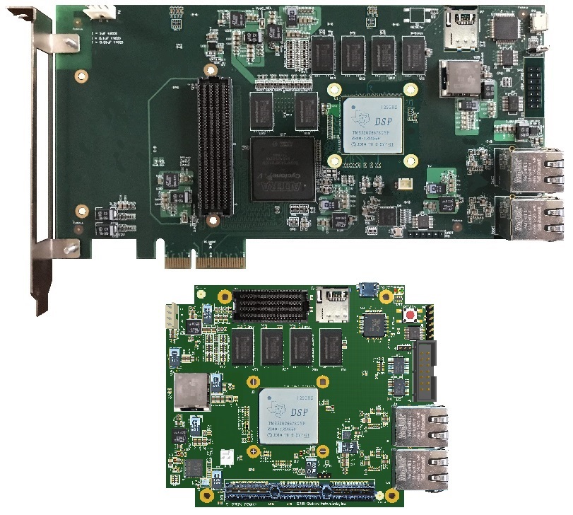
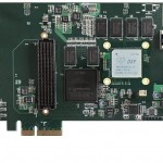 SI-C667xDSP-PCIe
 -
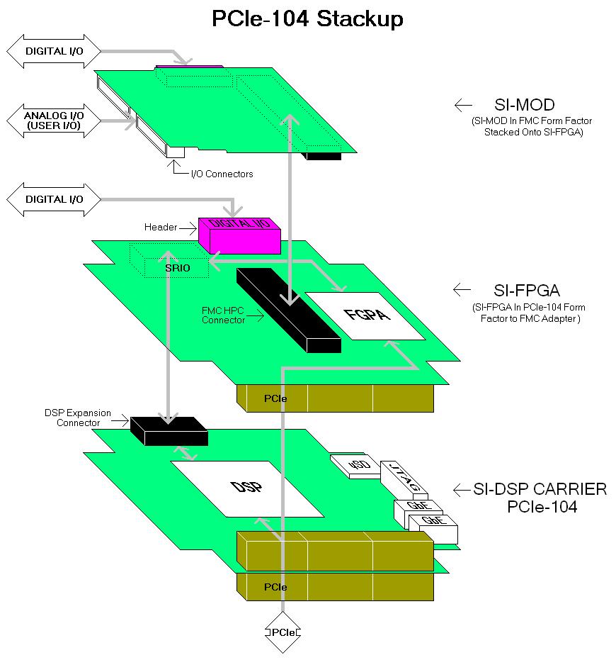
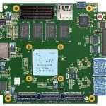 SI-C667xDSP-PCIe104
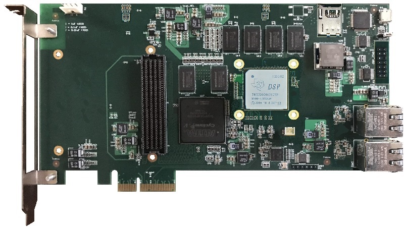
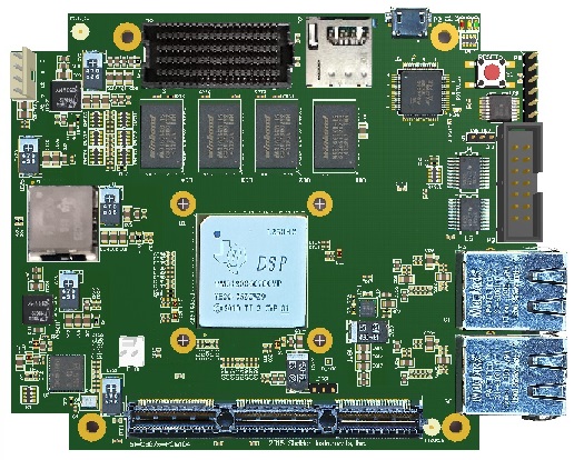
A powerful Keystone I Multicore Digital Signal Processor (DSP) card for the PCIe bus.
The SI-C667xDSP from Sheldon Instruments is a C programmable Digital Signal Processor (DSP) card with an FPGA bridge to an FMC expansion port, designed for low power environments that require intensive computing in a cost sensitive solution.
Keystone I devices supported on the SI-C667xDSP card:
TMS320C6678 (8 DSP CorePacs)
TMS320C6674 (4 DSP CorePacs)
TMS320C6672 (2 DSP CorePacs)
TMS320C6671 (1 DSP CorePac)
The SI-C667xDSP is a Small Form Factor (SFF) family of Commercial Off the Shelf (COTS) cards featuring the powerful Keystone I TMS320C667x DSPs from Texas Instruments, along with an optional Intel Cyclone V GX FPGA that interfaces to an FMC expansion port. The TI C667x DSPs are multicore DSP System on Chip (SoC), conveniently programmed using the C language. The number of C667x CorePacs range from one to eight, each clocked at 1.25GHz for a maximum of 320 GMAC and 160 GFLOP performance at a mere 10 watts of power consumption while most processors of this caliber are in the 40W-60W range.
Each DSP CorePac features 32K Bytes L1P, 32K Bytes L1D, and 512K Bytes of L2 of internal memory. Each level of cache can be programmed in blocks as SRAM or cache. The C667x chip also features a multicore shared memory controller that arbitrates 4M Bytes of shared SRAM memory between all cores and an external 64-bit DDR3 memory interface at 1333MHz.
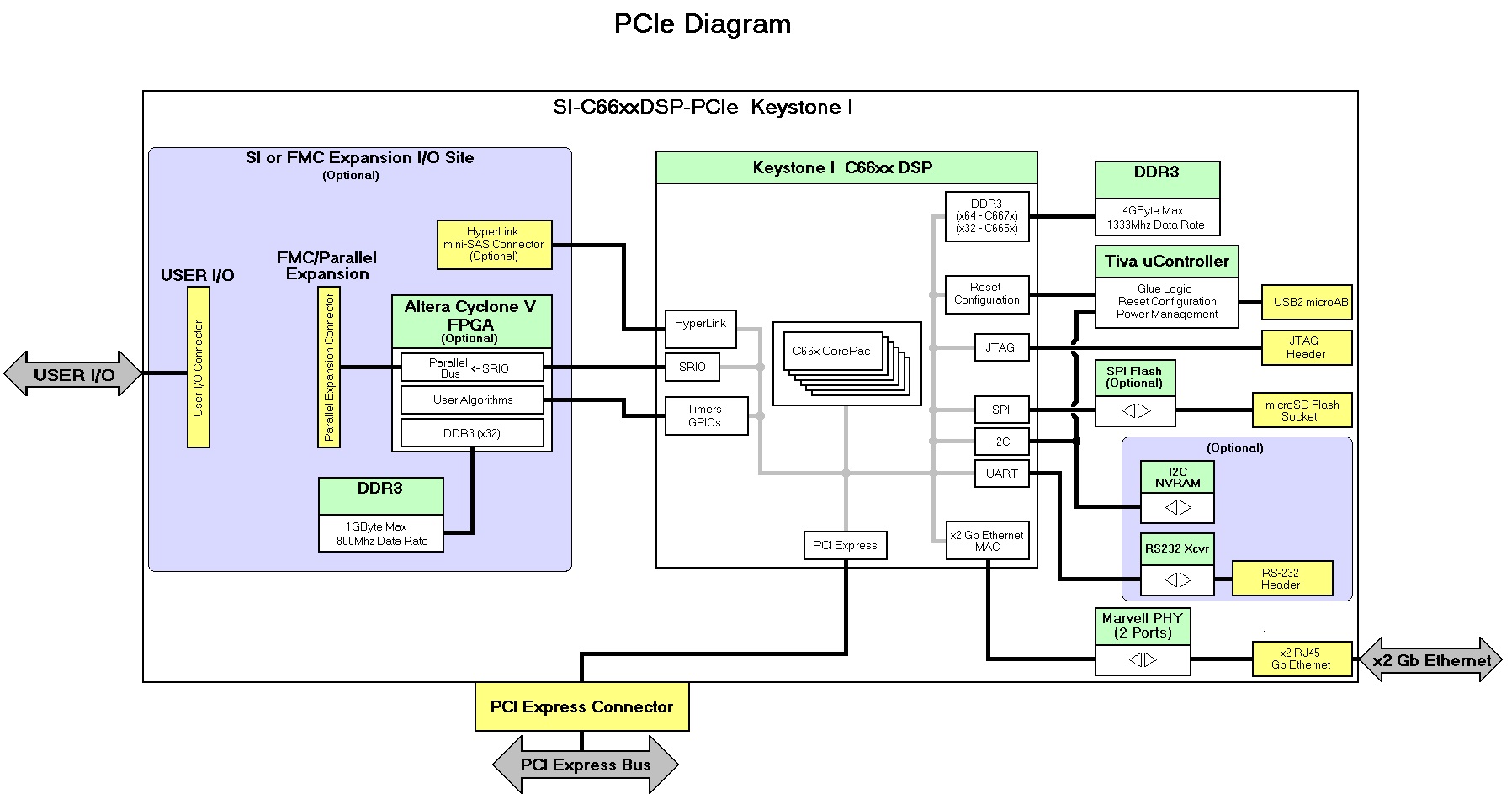
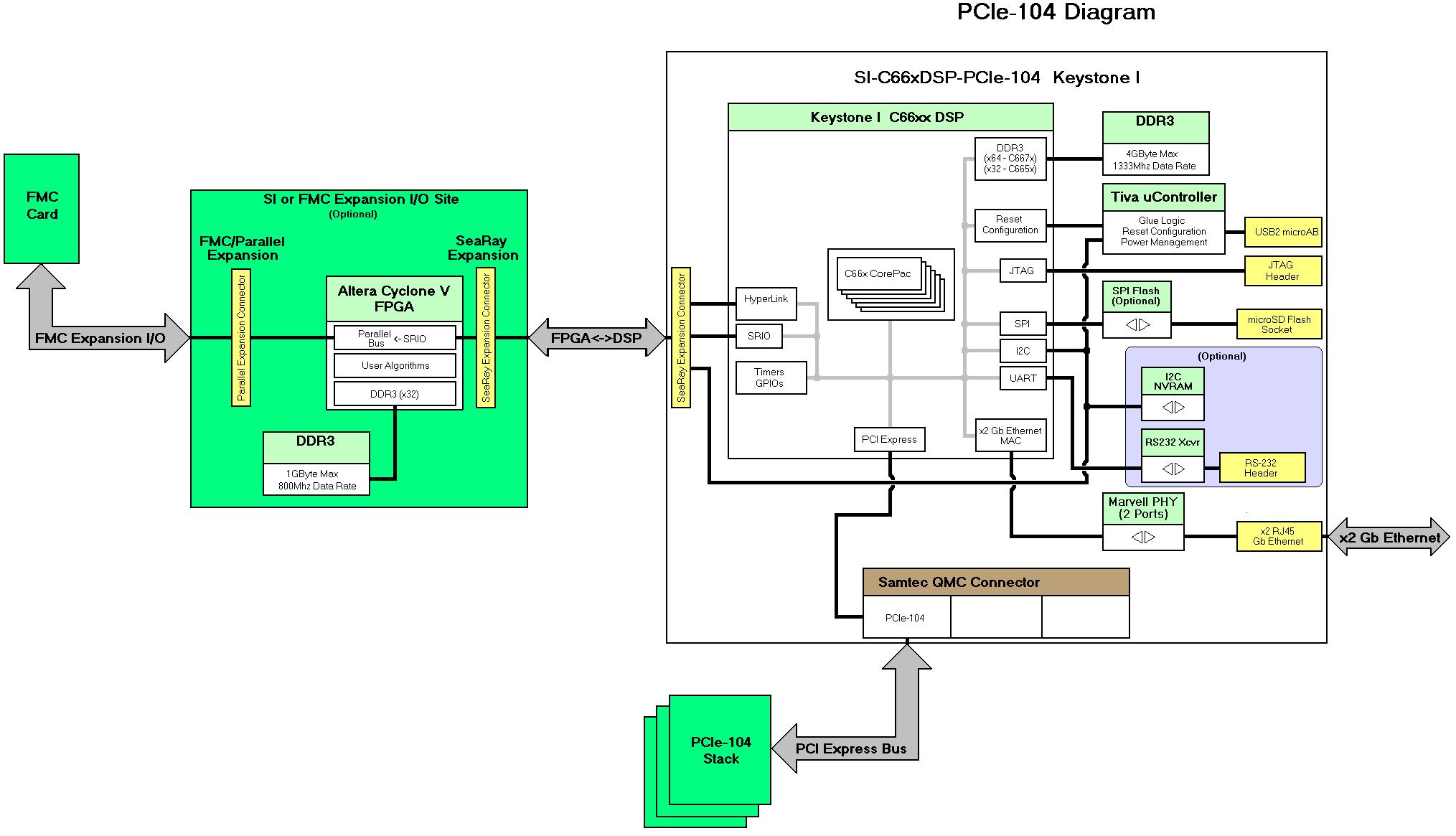
High Speed Serial Interfaces: GbE, PCIe, & SRIO
There are multiple high speed interfaces, with each capable of moving large amounts of data. The Gigabit Ethernet interface can take advantage of the on-chip Network Co-processor to offload most of the packet processing, thereby enabling full bandwidth utilization and freeing up the DSPs to perform the computations for which they were designed. A PCIe x2 Gen 2.0 interface provides connectivity to a system backplane or Thunderbolt cable, and the flexible SRIO 2.1 x4 5Gbps interface can be connected to either an optional FPGA or other external peripherals.
Hardware Expansion with FPGA & FMC Interface
The optional Altera Cyclone V GX FPGA includes SI’s proprietary IP layer that transparently translates SRIO so the FPGA may be used as an extra processing resource, as well as an expansion bridge to either an FPGA Mezzanine Card (FMC), or a legacy style parallel expansion bus – ideal for those who prefer to leverage a wide array of 3rd party FMC modules, their own custom hardware or simply update legacy designs with minimal effort.
Upgrades & Options
Upgrade options for the SI-C667xDSP include various core and memory configurations, nonvolatile storage, and either commercial or expanded temperature ranges. A full line of software development tools are available from Sheldon Instruments and TI for Windows and Linux platforms.
The SI-C667xDSP is available with extensive development tools from Sheldon Instruments, TI and Intel.
Host Side Tools
For the host PC side, Sheldon Instruments provides Windows/Linux 32/64 bit drivers, along with comprehensive sample application projects, with easy to use API libraries and related source code. The sample projects will be supplied as a command line utility, with a companion Qt GUI version. Its functionality includes:
DSP Side Tools
For the DSP side, TI offers Code Composer Studio Integrated Development Environment (CCS), and the Multicore Software Development Kit (MCSDK) that includes the Board Support Package (BSP), Chip Support Library (CSL), Network Development Kit (NDK), and Sys/Bios. Sheldon Instruments provides various TI CCS projects for the DSP, both compiled versions for quick loading with the host side sample program, along with complete projects and related source code. These DSP projects include:
There is important information for developers available from Texas Instrument’s website.
[table class=”siTB”]
Link, Description
Code Composer Studio IDE, Free download of Code Composer Studio IDE for Windows & Linux.
Keystone I Product Folder, Your main resource with links to data sheets; feature lists; user guides; application notes and software.
C6x Software Libraries, TI provides some really nice libraries for use on the C667x.
TMS320C667x DSP Math Library for Floating Point Devices, The DSP Math Library is a collection of optimized floating-point math functions for C programmers using the C667x devices. Both single and double precision floating point versions of these functions are available.
Test Reports, TI provides Test Reports to show how many cycles each function in the library requires to execute; very useful when trying to determine how many cycles are required to execute your overall algorithm and to determine points within the algorithm to break it up across multiple DSP cores.
TI-RTOS Networking, The TI NDK (Network Development Kit) combines dual mode IPv4/IPv6 stack with some network applications.
3rd Party Software, TI has a variety of software available that enables quick movement through the DSP application design process. Some of this software is free of charge; some needs to be purchased.
[/table]
FPGA and FMC Expansion Side Tools
For the optional FPGA that interfaces to the FMC interface, Intel offers the Quartus Prime Development Software that includes the free Lite Edition for the Cyclone V GX family. Sheldon Instruments provides various utilities FPGA projects and related source code which include:
There is important information for developers available from Intel’s website.
[table class=”siTB”]
Link, Description
Quartus Prime Lite Edition, Intel’s free design and development package for the Cyclone V GX series under Windows & Linux.
Cyclone V GX Product Folder, Your main resource with links to data sheets; feature lists; user guides; application notes and software.
[/table]
Keystone I C667x Processor and FPGA Resources
For more detailed documentation, check out the SI-C667x Keystone I Wiki Homepage.
Processor for SI-C667xDSP
[table class=”siTB”]
TI Keystone I TMS320C667x Family[attr colspan=”3″]
Number of Cores[attr rowspan=”4″], TMS320C6678, 8
TMS320C6674, 4
TMS320C6672, 2
TMS320C6671, 1
DSP Subsection (each C667x CorePac)[attr rowspan=”5″], Clocking, 1.25GHz
GMACS/GFLOPS, 44.8/22.4
L1 Program Cache/SRAM, 32KB
L1 Data Cache/SRAM, 32KB
L2 Cache/SRAM, 512KB
Shared[attr rowspan=”1″], L2 Cache/SRAM, 4MB
[/table]
External DSP Memory
[table class=”siTB”]
DDR3 Memory[attr colspan=”3″]
Port A[attr rowspan=”2″], Size, 512MB (64M x 64) to 2GB (256M x 64)
Speed, 667Mhz Clock Rate (1333Mhz Effective Data Rate)
[/table]
[table class=”siTB”]
Storage / Nonvolatile Memory[attr colspan=”2″]
SPI[attr rowspan=”2″], up to 64Mbit (8Mbx8) Flash
microSD flash card
I2C, up to 2KB EEPROM (inside Tiva uC)
[/table]
Optional Altera Cyclone 5 GX FPGA (PCIe Only)
[table class=”siTB”]
Resource, C3, C4, C5, C7, C9
Logic Elements (LE) (K), 31.5, 50, 77, 149.5, 301
ALM, 11900, 18868, 29080, 56480, 113560
Register, 47600, 75472, 116320, 225920, 454240
M10K, 1190, 2500, 4460, 6860, 12200
MLAB, 159, 295, 424, 836, 1717
Variable-preicision DSP Block, 51, 70, 150, 156, 342
18 x 18 Multiplier, 102, 140, 300, 312, 684
PLL, 4, 6, 6, 7, 8
SRIO Lanes @ 3.125Gbps, 2, 4[attr colspan=”4″]
BGA Package Density, 672 pins[attr colspan=”5″]
[/table]
Other Altera, Xilinx or Lattice devices also available on special request.
Optional External FPGA Memory (PCIe Only)
[table class=”siTB”]
DDR3 Memory[attr colspan=”2″]
Size, 256MB (64M x 32) to 1GB (256M x 32)
Speed, 400Mhz Clock Rate (800Mhz Effective Data Rate)
[/table]
High Performance Serial Interfaces
[table class=”siTB”]
Interface, Lanes, Speed
PCI Express Gen2[attr rowspan=”3″], Desktop PCIe: 2, 5 Gbps[attr rowspan=”3″]
PCIe-104: 1 or 2
Thunderbolt: 2
SRIO rev2.1, 4, 5 Gbps
Gigabit Ethernet, 1, 10/100/1000 Mbps
Optional Hyperlink, 4, 12.5 Gbps
[/table]
Port Connectors
[table class=”siTB”]
Port, Count, Connector Style
PCIe Gen 2[attr rowspan=”2″], 1[attr rowspan=”2″], Desktop PCIe: Edge connector (Endpoint)
PCIe-104: 3 segment Samtec QMS (Root Complex or Endpoint)
Ethernet, 2, RJ45s with integrated magnetics and LED indicators
microSD, 1, Standard socket for microSD/SPI flash
JTAG, 1, Keyed 14 pin (2×7) header; compatible with all third party emulators and debuggers
Optional Hyperlink[attr rowspan=”2″], 1[attr rowspan=”2″], Desktop PCIe: Optional mini-SAS HD+ 4i socket connector (Molex part number 76867-001; Mating cable is Molex 1110670200)
PCIe-104: Optional Searay connector to stack another SI-DSP carrier also equipped with a Hyperlink port
Optional Buffered UART, 1, 6 pin header
microUSB (Tiva uC), 1, microAB for card configuration
[/table]
[table class=”siTB”]
Optional Peripheral Expansion[attr colspan=”2″]
SRIO x4 lane Expansion[attr rowspan=”2″], Desktop PCIe: SRIO port directly connects to optional onboard FPGA which serves as a bridge to an FMC expansion connector
PCIe-104: SRIO port brought out to Samtec Searay/Q connector to stack a separate FPGA carrier equipped with its own FMC expansion connector
FMC/Parallel Expansion (available with FPGA option only)[attr rowspan=”2″], Single Width FMC site (HPC 400 pin connector)
User Defined I/O Signals: complete LA bus (34 differential pairs or 68 single ended I/Os); complete HA bus (24 differential pairs or 48 single ended I/Os); complete HB bus (22 differential pairs or 44 single ended I/Os). Note: Excludes all 10 multi-gigabit transceiver pairs which may be optionally included upon request with alternate Altera or Xilinx FPGA.
[/table]
Mechanical Properties
[table class=”siTB”]
Physical Dimensions/Electrical Requirements/Temperature[attr colspan=”2″]
Form Factor Dimensions[attr rowspan=”2″], Desktop PCIe (3/4 size): 9″/23cm(L) x 4.9″/12.5cm(W)
PCIe-104: 4.55″/11.6cm(L) x 3.775″/9.59cm(W)
Weight, 0.31lbs/140 grams
Supply Voltages, 3.3V @ 0.75A and +12V @ 1A
Power, 15 Watts typical; up to 25W with optional FPGA
Temperature, Commercial grade 0-85C. Consult factory for availability of industrial and military temperature grades
[/table]
PCIe Form Factor Cards
[table class=”siTB”]
Product, Description, Price (US dollars)
SI-C6678DSP-PCIe, TMS320C6678 – 8 DSP CorePacs, Call
SI-C6674DSP-PCIe, TMS320C6674 – 4 DSP CorePacs, Call
SI-C6672DSP-PCIe, TMS320C6672 – 2 DSP CorePacs, Call
SI-C6671DSP-PCIe, TMS320C6671 – 1 DSP CorePac, Call
[/table]
PCIe-104 Form Factor Cards
[table class=”siTB”]
Product, Description, Price (US dollars)
SI-C6678DSP-PCIe104, TMS320C6678 – 8 DSP CorePacs, Call
SI-C6674DSP-PCIe104, TMS320C6674 – 4 DSP CorePacs, Call
SI-C6672DSP-PCIe104, TMS320C6672 – 2 DSP CorePacs, Call
SI-C6671DSP-PCIe104, TMS320C6671 – 1 DSP CorePac, Call
[/table]
FPGA Options
[table class=”siTB”]
Product, Description, Price (US dollars)
-C3, x2 SRIO @ 3.125Gbps – 31k Gates, Call
-C4, x4 SRIO @ 3.125Gbps – 50k Gates, Call
-C5, x4 SRIO @ 3.125Gbps – 77k Gates, Call
-C7, x4 SRIO @ 3.125Gbps – 149k Gates, Call
-C9, x4 SRIO @ 3.125Gbps – 301k Gates, Call
[/table]