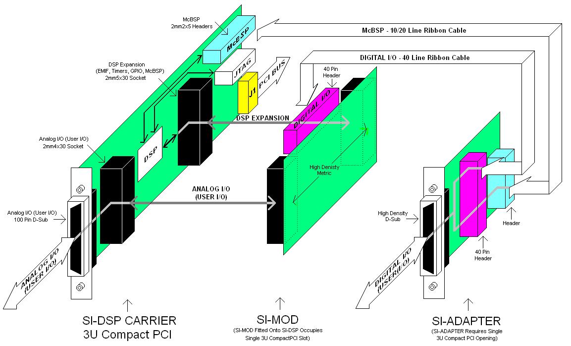
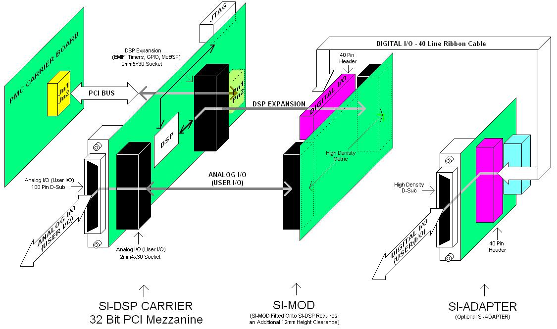
SI-MOD66xx
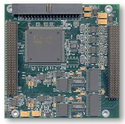
The SI-MOD66xx Expansion I/O Module.
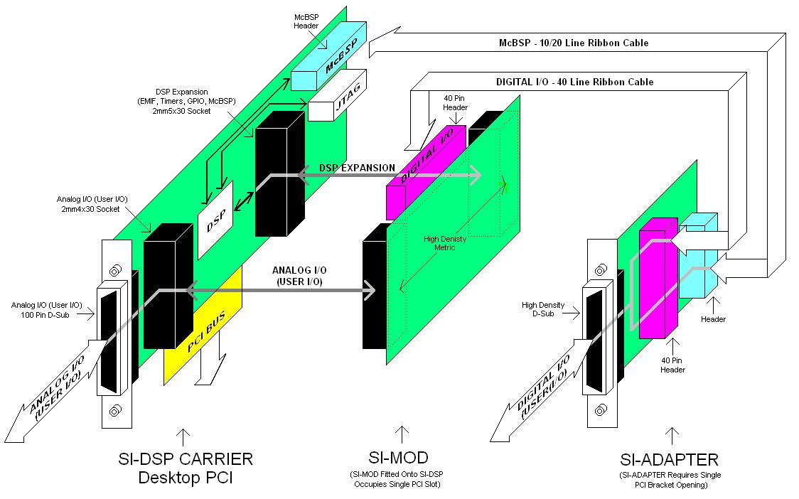
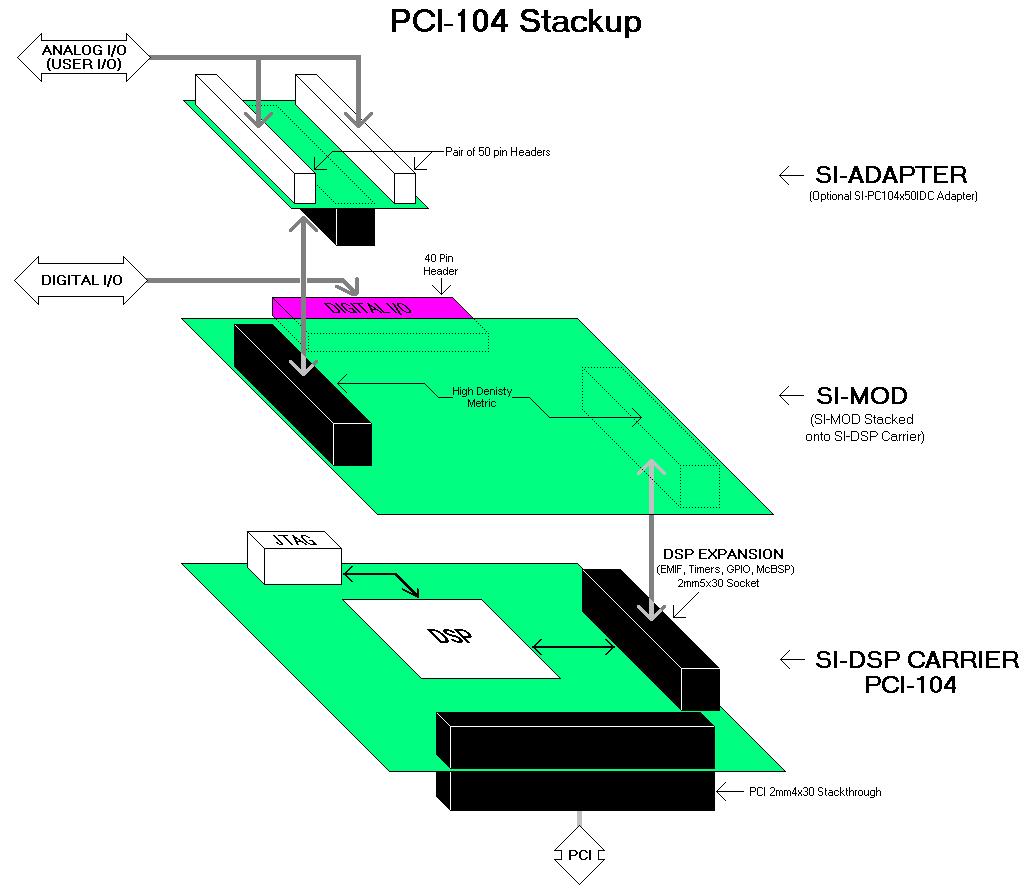
The SI-MOD66xx is a family of high resolution, multi function data acquisition and control modules that plug into any SI-CxDSP carrier processor card for the PCI bus.
Analog Inputs
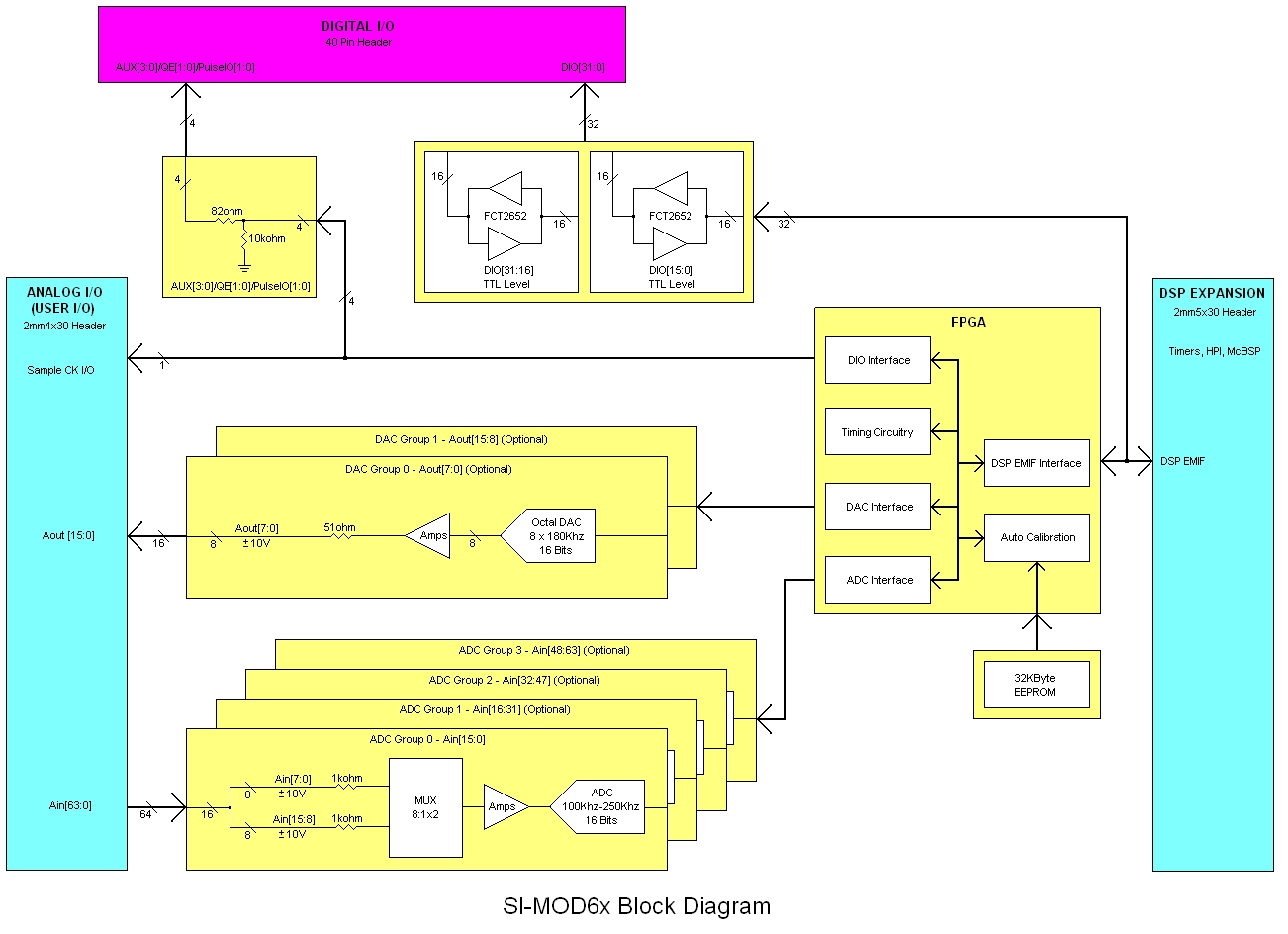
Each card features either 8DE/16SE, 16DE/32SE or 32DE/64SE analog input channels. Every group of 8DE/16SE channels is comprised of its own multiplexer, programmable gain instrumentation amplifier and ADC circuitry. Up to four (4) distinct channels, one from each group, can be simultaneously sampled. The ADC resolution is 16 bits, each with sampling rates ranging from 0hz to 100khz/250khz, or an additive rate of 400khz/1Mhz respectively. The maximum input voltage level is between ±10Vp (or ±9.5Vp for the “HG” or high gain option), with gains controlled by a precision differential instrumentation amplifier ranging from 1, 2, 5, 10, along with an optional 20, 50, and 100 for the “HG” option. The ADCs are based on a Successive Approximation architecture, which makes them ideal for control applications. Each input’s termination can be individually programmed for differential or single ended operation, thereby not limiting you to an all-or-nothing configuration.
Analog Outputs
Additionally, up to sixteen (16) analog outputs can each update at rates up to 180khz, with 16 bits of resolution. These bipolar outputs have a maximum ±10Vp range, along with a 1-pole smoothing filter.
Digitally Controlled Calibration
An on board 32KByte EEPROM contains the offset and gain errors which are loaded into the FPGA and used to implement real time digital calibration on all analog I/O.
Timing
The sample clock can be derived internally or externally. If derived internally from the onboard timing circuitry, either several traditional divide by N counters or a pair of onboard Direct Digital Synthesizers (DDSes) may be used. The DDSes provide programmable sampling rates with precision up to ±1hz resolution. An externally sourced sample clock can also be used to accommodate a variety of sampling schemes. All ADC sample clocks are routed to an external connector in the case that multiple cards need to be synchronized to a common clock.
Digital I/O
Thirty six (36) general purpose, highly flexible digital I/O lines are also available, with thirty two (32) lines configured as a pair bidirectional, buffered 16 bit ports, and the other four (4) which can also double as a pair of Quadrature Encoder inputs, or as a set of four (4) individual Pulse I/Os lines. These lines are in addition to any of the digital I/O lines native to the DSP carrier card, such as its own serial ports and timers.
All functions for the SI-MOD66xx are fully programmable with QuVIEW and QuBASE, which are a set of DSP-resident libraries for real time performance that greatly accelerate data acquisition, signal processing, and control applications. QuVIEW is a real time accelerator for LabVIEW, and QuBASE a real time accelerator for Visual Basic. A full range of examples and tutors are provided to demonstrate their ease of use and breadth of functionality and capabilities. Complete driver support for Windows and Linux.
For more detailed documentation, check out the SI-MOD66xx Wiki Homepage
DSP interface
[table class=”siTB”]
Expansion Interface[attr colspan=”2″]
Interface to DSP Expansion, Parallel 32 bit data and 16 bit address
Clock Speed, up to 40Mhz or half of DSP’s parallel expansion bus clock
[/table]
Analog Inputs
[table class=”siTB”]
Analog Input Section[attr colspan=”2″]
Input Termination Options [attr rowspan=”4″], SI-MOD6616-250: 16S/8D; 0hz to 250khz additive sampling for all channels
SI-MOD6632-250: 32S/16D; 0hz to 500khz additive sampling for all channels
SI-MOD6600-250: 64S/32D; 0hz to 1Mhz additive sampling for all channels
Flexible input termination: each channel individually programmable for differential or single ended operation
MUX-PGA-ADC grouping, Up to 4 distinct groups simultaneously sampled; up to 16 channels per MUX-PGA-ADC group (4 x16 = 64 channels maximum)
Multiplexer Circuit, 4:1×2 MUX p/n DG409
Input Characteristics [attr rowspan=”3″], Voltage Level: ±10Vp maximum
Impedance: minimum 1Mohm
Coupling: DC
Amplifier Gains, 1; 2; 5; 10; 20; 50; 100 p/n LTC6910-1 (Linear Technology)
Sample Rate, Each MUX-PGA-ADC group has 0hz to 250khz muxed time division sampling on 16 channels; for a maximum additive rate of 1Mhz on all channels
ADCs, Successive Approximation ADCs with 16 bits of resolution; 250khz additive sampling; p/n LTC1864 (Linear Technology)
[/table]
Analog Outputs
[table class=”siTB”]
Optional Analog Output Section[attr colspan=”2″]
Options [attr rowspan=”2″], -8DAC: 8 Analog Outputs
-16DAC: 16 Analog Outputs
DAC Circuit, p/n LTC2600 (Linear Technology)
Update Rate, 0hz to 180khz per channel
Output Voltage Level, Bipolar: ±10Vp maximum
Output Smoothing Filter, Fixed 39khz 1-pole lowpass smoothing filter.
[/table]
Timing
[table class=”siTB”]
Timing Section[attr colspan=”2″]
Timing elements[attr rowspan=”3″], 2 internal DDSes; 27 bit resolution phase accumulators
4 internal programmable Event Counters; based on divide-by-n 32 bit resolution counters
Flexible switching matrix allows timing signals to be routed from onboard resources as well external sources (Quadrature Encoders; Pulse I/Os)
[/table]
Digital I/O
[table class=”siTB”]
Digital I/O Section[attr colspan=”2″]
36 General Purpose Discrete I/O[attr rowspan=”2″], 32 line bi-directional port with programmable directional control as two individual 16 bit ports. Nominal 3.3V CMOS/TTL logic levels (5V IO tolerant); directly tied to 74FCT2652 class of bidirectional buffers
4 lines reconfigurable as general purpose I/Os or as a pair of Quadrature Encoder inputs or as 4 bidirectional Pulse I/O lines. Nominal 3.3V CMOS logic levels; directly tied to Xilinx Spartan 3E FPGA
[/table]
General Features
[table class=”siTB”]
General Features[attr colspan=”1″]
Xilinx XC3S500E Spartan 3 FPGA
On board 32KByte EEPROM contains offset/gain errors; loaded to FPGA for real time digital calibration on all analog I/O
Internal and external hardware triggers and sample clocks; software triggers
Fully programmable with QuVIEW (an accelerator library for LabVIEW) and QuBASE (an accelerator library for Visual Basic)
Full suite of development tools from Sheldon Instruments
Windows and Linux 32/64 bit application and driver support
[/table]
Mechanical Properties
[table class=”siTB”]
Physical Dimensions/Electrical Requirements/Temperature[attr colspan=”2″]
Dimensions, 3.7″/9.4cm(L) x 3.7″/9.4cm(W)
Weight, 0.18lbs or 85 grams
Supply Voltages[attr rowspan=”3″], +3.3Vdc for logic circuitry (+1.2Vdc and +2.5Vdc generated with onboard regulators)
+5Vdc for 32 bit port buffers
±12Vdc for analog circuitry
Power[attr rowspan=”2″], 7 Watts typical with minimum configuration: +12Vdc@0.25A; -12Vdc@0.2A; +5Vdc@0.1A; +3.3Vdc@0.35A
14 Watts typical with maximum configuration: +12Vdc@0.55A; -12Vdc@0.5A; +5Vdc@0.1A; +3.3Vdc@0.35A
Temperature, Commercial grade 0°-85ºC. Consult factory for availability of industrial and military temperature grades
[/table]
Multifunction I/O Module with 250kHz ADCs
[table class=”siTB”]
Product, Description, Price (US dollars)
SI-MOD6616-250, 8D/16S analog in – x1 SAR 16 bit ADC @250Khz – gains 1 to 100 – 36 digital I/Os, 695
SI-MOD6632-250, 16D/32S analog in – x2 SAR 16 bit ADC @250Khz – gains 1 to 100 – 36 digital I/Os, 795
SI-MOD6664-250, 32D/64S analog in – x4 SAR 16 bit ADC @250Khz – gains 1 to 100 – 36 digital I/Os, 995
[/table]
DAC Options for SI-MOD66xx
[table class=”siTB”]
Option, Description, Price (US dollars)
-8DAC, Add “-8DAC” to part number. x8 analog outputs, 125
-16DAC, Add “-16DAC” to part number. x16 analog outputs, 225
[/table]